Antenna matching – a simple explanation of the procedure
Nowadays, it is almost impossible to imagine a world where our lives are not supported by smart devices at home, on the go, in the office and during leisure time. Devices are becoming increasingly networked for this purpose, which is referred to as the "Internet of Things" (IoT). Reliable connectivity forms the backbone of this. From intelligent sensors to industrial control systems, IoT devices need a robust and efficient way to transmit data through wireless networks. There are different standards for IoT devices, such as LTE Cat M1 (LTE-M), NB-IoT or LoRaWAN, which have been developed specifically for these uses.
A key aspect of wireless communication is the transfer of signals from the electronic devices into the air, which is done with a suitable antenna. And yet, it is not only the antenna, but also its installation, the immediate surroundings and the wiring that are crucial here.
This blog post describes design considerations and the process of the matching network design for optimising LTE Cat M1 antennas. As a result, the range can be significantly enhanced and energy requirements reduced.
Why is antenna matching necessary?
The efficiency of signal transmission between an antenna (load) and a radio module (source) is fundamentally dependent upon the consistency of their impedances. Antenna matching is therefore about impedance matching. In RF applications, this is typically 50 ohms. Variations in impedances lead to signal reflections resulting in performance losses and inefficient transmission. While the antennas are usually tuned to 50 ohms impedance by the manufacturer, the impedance changes in the real world due to environmental influences. These may be caused by different materials in the vicinity of the antenna, electronic components in the antenna path, the PCB or the positioning of the antenna.
A matching network is used to correct this impedance difference, which consists of passive electronic components such as inductors, capacitors and, in some cases, resistors. These components are placed in the antenna path between the radio module and the antenna. The impedance of the antenna can be adjusted through correct topology and dimensioning of the components.
S11 return loss measurement and the Smith chart
Impedance is calculated by an S11 measurement with a VNA (Vector Network Analyser). The results are usually represented on the Smith chart and as a log-magnitude diagram.
When taking the measurement, a point is plotted on the Smith chart for each frequency. The Smith chart is a visualisation of impedances and reflections as imaginary and real parts. The distance between the frequency point and the centre of the Smith chart corresponds to the attenuation. A greater distance from the centre means more reflection and correspondingly lower transmitted signal power.
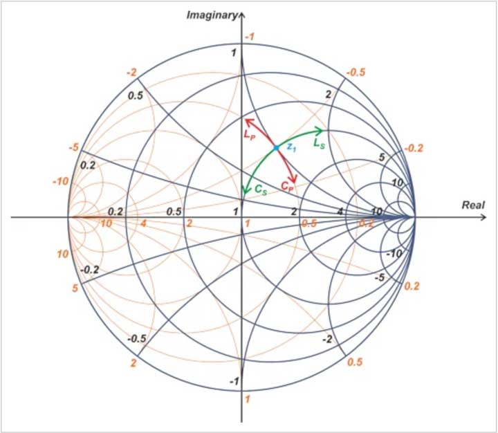
The centre of the Smith diagram corresponds to an impedance of 50 ohms, where the attenuation is -∞ dB. The aim is to bring the frequency points as close to the centre as possible. This can be achieved by using serial or parallel components in the antenna path:
- Serial components rotate the frequency point around the real axis = ∞ point on the right side (grey lines)
- Parallel components rotate the frequency point around the real axis = -∞ point on the left side (orange lines)
For example, point Z1 in Figure 1 could be moved towards the centre with a serial capacitor (C). It should be noted that all frequency points are influenced by one component in the RF path. Thus, modification means that an additional frequency point can be removed from the centre. An optimal compromise has to be found.
Figure 1: Example Smith-Chart
Antenna selection and design considerations
There is a wide selection of antenna types, each with their advantages and disadvantages, such as dipole, patch/chip, omnidirectional or directional antennas. All antennas work with different frequency bands. In our experience, either a dipole antenna is used as a flex print or a patch antenna as part of the PCB in many cases.
The following basic considerations should be taken into account as a bare minimum when selecting the antenna:
- Datasheet parameters vs. parameters under real conditions
The parameters specified in the datasheet (e.g. VSWR) should be considered as an ideal case under laboratory conditions. Under real conditions, the parameters will deviate. - Required frequencies
The more broadband the antenna is, the more compromises have to be made. - Space within the housing
Large antenna layout and shorter vs. small antenna layout and taller.
For example, patch antennas are very flat and the antenna itself is also small, but a large area of ground around the antenna is required and this results in a large layout.
As a general rule, the lower the frequency, the larger the antenna. - Housing material
Manufacturers optimise certain antennas for given materials. - Reproducibility during assembly
Variations in the assembly have an impact on the impedance and thus on the performance. Small changes, such as a cable being routed differently in the device or an antenna being attached at an angle, can significantly alter the impedance of the antenna. Close collaboration between hardware development, design and production is crucial.
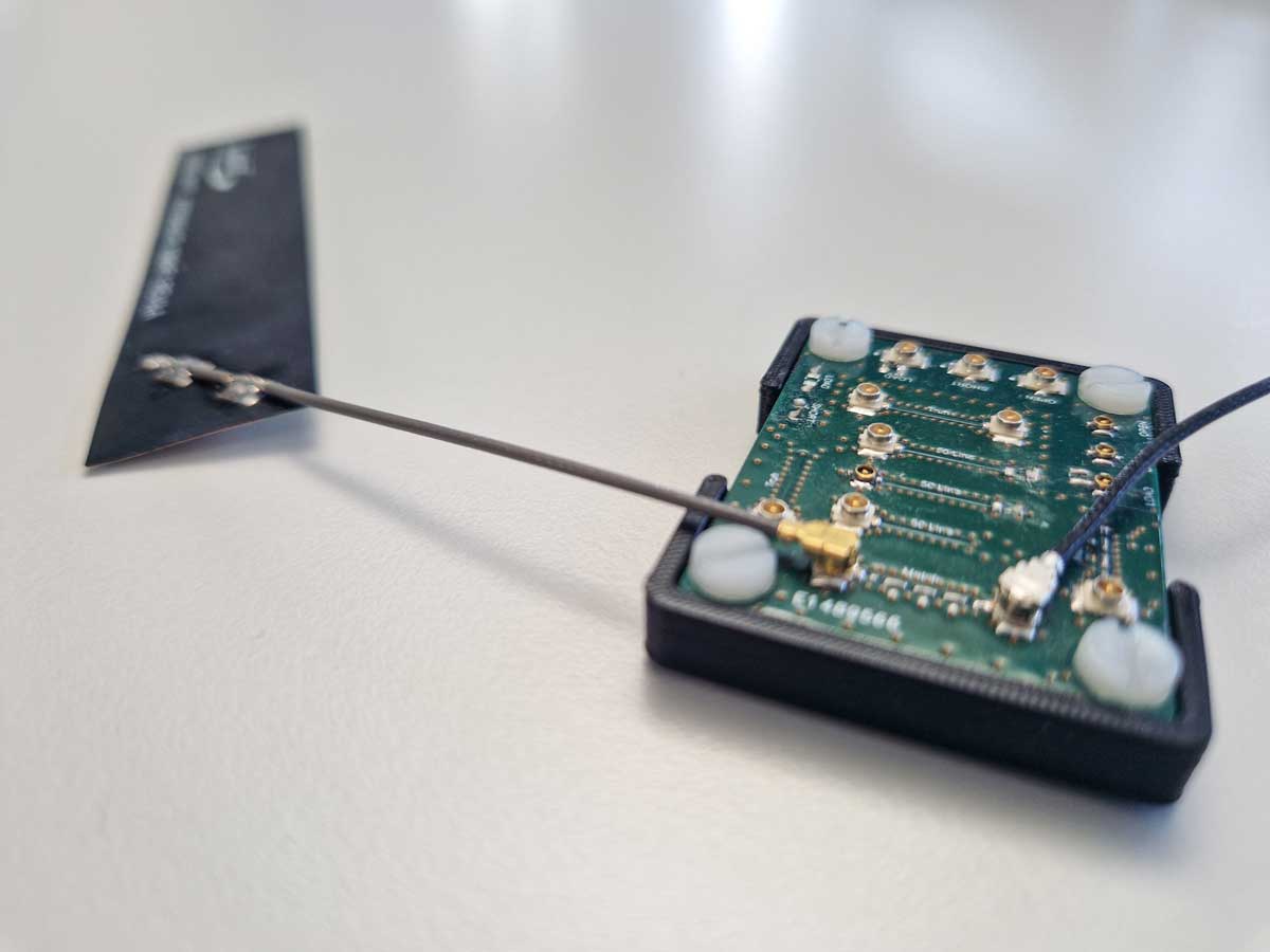
Antenna path alignment workflow (matching network)
In principle, the return loss should be as low as possible. Practice has shown that broadband antennas work with a maximum return loss of -6 dB (VSWR < 3:1). For narrowband antennas, such as GPS, the target should be a maximum return loss of -10 dB (VSWR < 2:1).
To evaluate the matching network, the following components must be physically available:
- Antenna
- Electronics
- Housing
- Cabling/assembly determined
If these requirements are met, the process outlined below can be used to evaluate the matching network. It should be noted that this is an iterative process and that the individual steps sometimes require several runs.
- Acquire the touchstone file with VNA
- Set up the simulation (e.g. with Qucs Studio)
- Verify the simulation
- Optimise the matching network in simulation
- Equip with inductors and capacitors according to the optimised simulation
- Take the test measurements
- Gradually adjust the matching network according to Smith chart
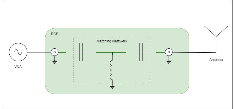
Return loss measurements are taken with a VNA. The complete RF path should be measured:
Figure 2: RF path with π network impedance matching topology
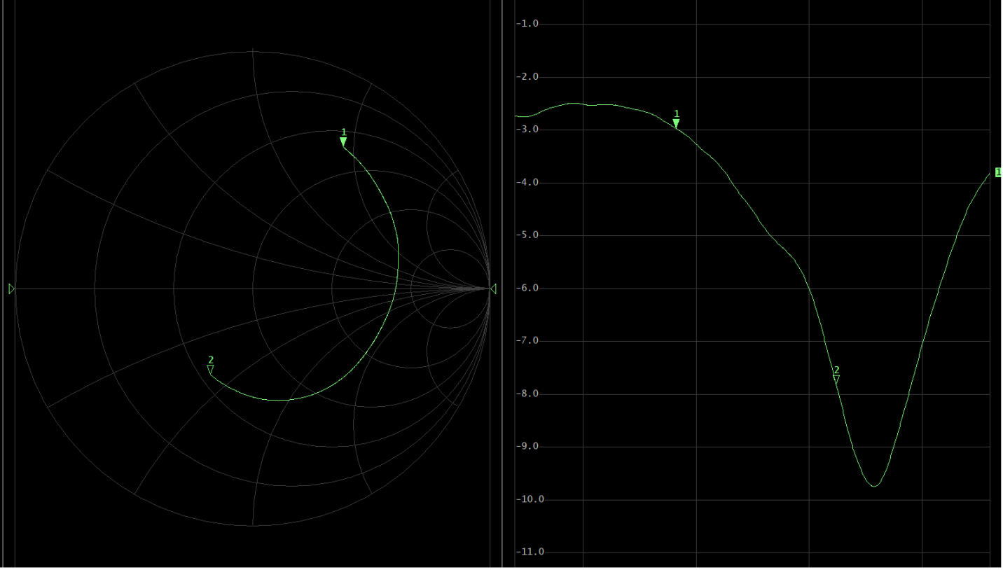
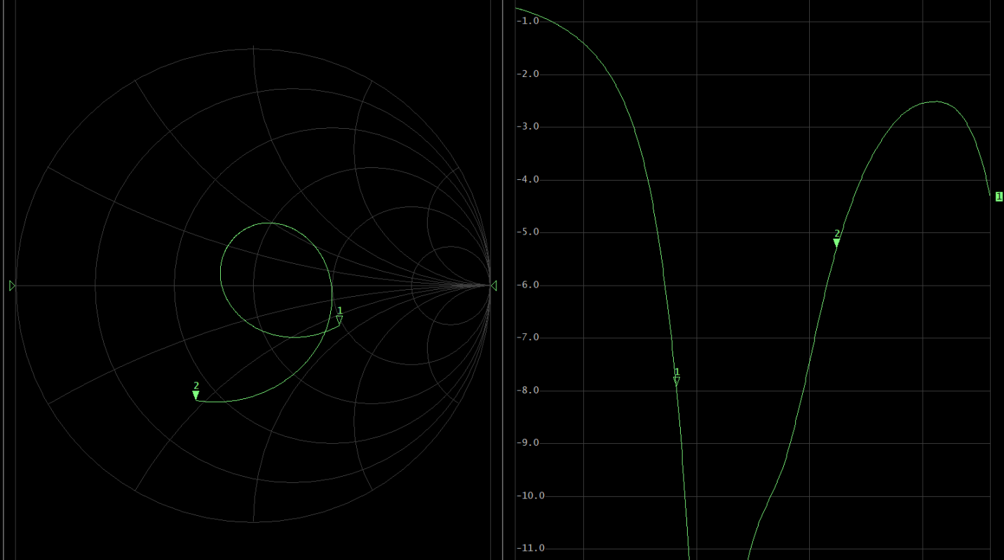
In the following example, the return loss of the antenna could be significantly improved with a matching network, which has been optimised according to the process mentioned above. Between the markers (frequency band), the S11 could be reduced on average from -5 dB to -9 dB. This improvement increased the range of the antenna by several kilometres.
Figure 3 left: S11 without matching / Figure 4 right: S11 with matching
Conclusion
Optimising antennas with an impedance matching network is crucial for efficient signal transmission in the IoT. Precise design, evaluation and optimisation can significantly improve the performance and range of the antennas. While the development process is time-consuming and requires a great deal of expertise, more reliable connectivity and efficient data transmission are essential in the world of IoT.
RF applications require specific knowledge and equipment. CSA Engineering has supported or taken over the development and/or optimisation of radio applications in several projects for various clients.
We would be happy to help you implement your plans too.